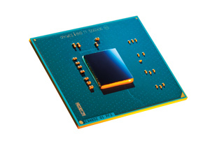
How do mobile devices keep get faster, thinner, and more power efficient? It’s thanks to the quick advances in chip manufacturing, which help churn out smaller chips packed with new features.
The next round of premium smartphones early next year could feature chips like Qualcomm’s Snapdragon 835, made using the latest, 10-nanometer process.
Continuing with the famous Moore’s Law observation, it’s likely that two years after that, smartphones will get even faster and smaller chips will be made using a 7-nanometer process.
On Monday, ARM, with its chip designs in most smartphones, said it is working with prominent chip manufacturer TSMC (Taiwan Semiconductor Manufacturing Co.) to make 7nm chips. ARM shared intellectual property for its 7nm designs, allowing chips to be designed for manufacturing in TSMC’s factories.
The manufacturing of chips on TSMC’s 7nm process is expected to start in 2018, said Ron Moore, vice president of marketing for ARM’s physical design group.
In ARM’s trials, the 7nm chips will provide a 15 to 20 percent speed boost compared to chips made using TSMC’s 16nm process. Smartphone chip makers could tweak the architecture to bring even better performance to the chips.
ARM-based chips for servers and IoT devices will also be made on the 7nm process. Ultimately, only the chipmakers using ARM designs will be able to provide metrics on performance improvements based on the tweaks they made, Moore said.
Applications like virtual reality and machine learning are demanding more performance out of chips. The ARM manufacturing IP provided to TSMC solves some challenges around memory, power distribution, and moving data in and out of memory.
For example, many customers are planning multi-GPU configurations for servers in the cloud or for machine-learning infrastructures. The chip IP provides data path optimizations so data can travel quickly within these infrastructures and at the right power consumption levels.
Many advances are expected on the 7nm process, including EUV (extreme ultraviolet) that allows for finer details to be etched on chips. Chips designed with the ARM’s IP won’t require designers to have deep knowledge about the underlying manufacturing technologies, Moore said.
TSMC rival Globalfoundries is also moving to the 7nm process, and production could start in 2018. Samsung hasn’t publicly talked about its 7nm plans. Intel says it has “visibility” of 7nm, meaning it is on the company’s roadmap, but hasn’t talked about when it will be implemented.
The next step beyond -nm is the 5nm process, which will be discussed at the International Electron Devices Meeting next week in San Francisco. Participants will also discuss silicon replacement materials. Samsung will discuss the merits of silicon germanium, and participants will also examine other exotic materials.
Intel is already planning to use III-V materials, based on elements from the third and fifth columns of the periodic table, like gallium-arsenide, in forthcoming chips. Gallium arsenide is a better electricity conductor than silicon, and it could add to the power efficiency of chips.


